
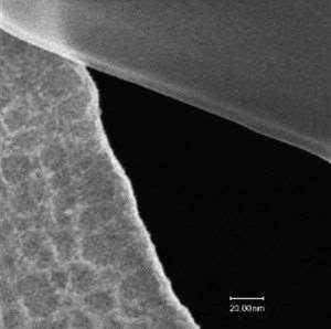
For demonstration of the image resolution of 0.24 Nanometers a linescan over the very sharp edge of an asbestos fiber on a thin holey carbon foil is shown. The texture of the holey carbon foil demonstrates the extremely high surface sensitivity of t
The new benchmark is also claimed to be three times better than the most sophisticated scanning electron microscopes are able to achieve today with the same surface sensitivity, according to senior vice president Dr. Nicholas P. Economou.
The secret behind the extreme high resolution of the Helium-ion microscope is said to lie in the proprietary source technology and in the interaction between the scanning ion beam and the surface of the specimen.
The source of the microscope is very small and the helium ions emanate from a region as small as a single atom.
Unlike electrons, the helium ions have a very small wavelength and hence do not suffer appreciably from adverse diffraction effects – a law of physics which fundamentally limits the imaging resolution of electrons.
Also, the helium ion beam triggers signals directly from the surface of the sample and stays very collimated upon entering the sample.
This results in very sharp and surface sensitive images at the quoted resolution which can be easily interpreted.
In contrast, for a typical scanning electron microscope (SEM), the majority of the secondary electrons that are used for imaging come from deeper and much less confined regions within the sample, creating blurrier images with less resolution than the Helium-ion microscope, Economou said.
“Some layers of integrated circuits already have reached a thickness of only a few atoms”, added Dr. Rainer Knippelmeyer, senior VP of operations at Carl Zeiss SMT.

.jpg&h=140&w=231&c=1&s=0)

.jpg&h=140&w=231&c=1&s=0)

.png&w=100&c=1&s=0)


 iTnews State of Data & AI Breakfast
 Forrester's AI Forum Sydney
 The 2026 iAwards
.jpg&w=120&c=1&s=0) Integrate 2026
Integrate 2026
 Security Exhibition & Conference


_(1).jpg&h=140&w=231&c=1&s=0)


