US researchers have successfully assembled a tiny processor from nanometre-scale components to perform basic arithmetic and logical functions.
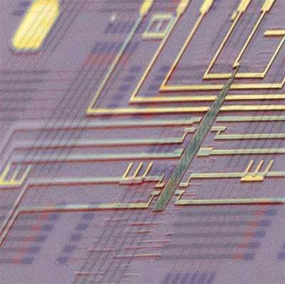
Harvard University's Charles M. Lieber and his team built 960μm2 (square micrometre) 'logic tiles' that could perform adder, subtractor, multiplexer, demultiplexer and clocked D-latch functions.
The tiles each contained 496 programmable transistors built from ten-nanometre-thick germanium wires, and were touted as a "world first" in complexity and function.
In a research paper published in Nature today, the researchers described designing, constructing and using the programmable tiles.
"For the past 10 to 15 years, researchers working with nanowires, carbon nanotubes, and other nanostructures have struggled to build all but the most basic circuits, in large part due to variations in properties of individual nanostructures," stated Lieber, who collaborated with the MITRE Corporation on the project.
"This work represents a quantum jump forward in the complexity and function of circuits built from the bottom up.
"[It] thus demonstrates that this bottom-up paradigm, which is distinct from the way commercial circuits are built today, can yield nanoprocessors and other integrated systems of the future."
Since each tile had a maximal voltage gain of ten and could match input-outage voltage levels, they could be arranged into linear or tree-like interconnected arrays, the researchers wrote.
In the near term, the technology could yield simpler, low-power, application-specific 'nanocontrollers' for use in tiny embedded systems and biomedical devices, they suggested.
Lieber acknowledged in Nature News that the chip would struggle to compete with conventional electronics, which crammed far more transistors onto a single chip.
Each of Harvard's nanotransistors occupied 1.9μm2 - more than twenty times the 0.09μm2 area required by logic gates in current 32nm CMOS chips, the researchers wrote (pdf).
The Intel Sandy Bridge, which launched in Australia last month, fit each of its 995 million transistors into a 0.217μm2 area, with a total area of 216mm2 (square millimetres).
Lieber and his team said their chip could be further improved to be up to 100 times more efficient than current electronics, and require only 0.0017μm2 per transistor.

.jpg&h=140&w=231&c=1&s=0)

.jpg&h=140&w=231&c=1&s=0)
.png&w=100&c=1&s=0)


 iTnews State of Data & AI Breakfast
 Forrester's AI Forum Sydney
 The 2026 iAwards
 Security Exhibition & Conference
.jpg&w=120&c=1&s=0) Integrate 2026
Integrate 2026


_(1).jpg&h=140&w=231&c=1&s=0)