iTnews
  • Home
  • News
  • Technology
  • Hardware

IBM develops nano-manufacturing technique

By Liz Tay
Apr 23 2010 5:42AM
Follow google news

Heated silicon tip etches nanoscale designs.

IBM researchers have developed a manufacturing technique capable of etching 1,000 three-dimensional world maps on materials the size of a grain of salt.

IBM develops nano-manufacturing technique

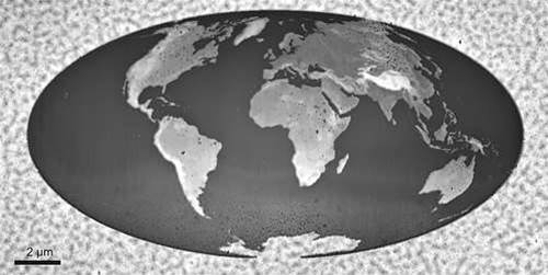
The technique involved a tiny, silicon 'scanning probe' that measured 500nm (nanometres) long and 5nm thick and was heated above 330 degrees Celsius.

As it came in contact with substrate materials -- called resists -- the probe would cause the material to evaporate, thereby etching patterns on the material.

Reaching a resolution of 15nm, the technique could enable future nanoelectronic devices to be produced more cheaply and efficiently than state-of-the-art electron beam lithography (EBL) systems.

According to IBM, potential applications ranged from fast prototyping for CMOS nanoelectronics to fabricating shape-matching templates for self-assembling nano-rods or nano-tubes.

IBM physicist Michel Despont explained that the technique required fewer processes than EBL systems, and would cost five times less to perform the same task.

But the real breakthrough was its ability to create complex 3D patterns and structures, which could enable new micro-optic devices, he said.

"We believe that the fact that you can do 3D patterning will open up applications that we haven't thought of before," Despont told iTnews.

Ian Boyd, who is the director of the Melbourne Centre for Nanofabrication (MCN), explained that EBL was unsuitable for the mass manufacture of nanotechnology as it could only target a small area at a time.

When it officially opens in July, the Centre will house a $2.5m EBL tool said to be the first of its kind in Australia.

"The resolutions available for EBL are of the order of 10nm at the moment," Boyd told iTnews.

While several instances of the simpler scanning probe technique could be run in parallel to pattern larger areas of substrate, the same could not be said for EBL as nearby electron beams would likely interfere with each other.

Boyd said manufacturing nanoelectronics with EBL would be akin to "ploughing a field with a knitting needle".

Meanwhile, Despont said IBM's technique would not be mature enough for its commercial effects to be apparent for at least five years.

The technique was two years in the making and represented a collaborative effort between Despont's team of physicists and chemists who developed the substrate materials at IBM Research in Almaden.

In the near future, the researchers would focus on making the technology available to universities and other corporate research laboratories. They were in discussions with a European manufacturing company about commercialisation.

"We believe that if this technology has a future, we will need to have a large research community working on it," Despont told iTnews.

Add iTnews as your trusted source

Add iTnews As Your Trusted Source Add iTnews As Your Trusted Source
Got a news tip for our journalists? Share it with us anonymously here.
Tags:
hardwareibmmanufacturenanotech

Related Articles

  • Kmart Group to expand RFID tagging to more products and to Target Kmart Group to expand RFID tagging to more products and to Target
  • Microsoft teases new era of AI-driven devices Microsoft teases new era of AI-driven devices
  • PsiQuantum to build computer at Moreton Bay PsiQuantum to build computer at Moreton Bay
  • US to invest in IBM, other quantum computing firms US to invest in IBM, other quantum computing firms
Join our WhatsApp Channel

Partner Content

From test case to control tower: How DXC and ServiceNow are governing enterprise AI at scale
Promoted Content From test case to control tower: How DXC and ServiceNow are governing enterprise AI at scale
CommBank creates opportunities for technologists to upskill  with frontier AI companies
Partner Content CommBank creates opportunities for technologists to upskill with frontier AI companies
You meet the security standard. Shame no one can see it
Promoted Content You meet the security standard. Shame no one can see it
The hidden economics of AI: Why token usage matters more than you think
Partner Content The hidden economics of AI: Why token usage matters more than you think

Sponsored Whitepapers

Are Australian organisations as cyber-ready as they think?
Are New Zealand organisations as cyber-ready as they think?
From visibility to execution:  Fixing the SaaS management gap
From visibility to execution: Fixing the SaaS management gap
When cyber risk has no clear owner: A practical guide for senior Australian business leaders
Agile in the AI Era: why projects still fail

Events

  • iTnews State of Security Breakfast iTnews State of Security Breakfast
  • iTnews State of Data & AI Breakfast iTnews State of Data & AI Breakfast
  • Forrester's AI Forum Sydney Forrester's AI Forum Sydney
  • The 2026 iAwards The 2026 iAwards
  • Security Exhibition & Conference Security Exhibition & Conference
Share on Facebook Share on LinkedIn Share on Whatsapp Email A Friend

Most Read Articles

Google says it has cracked a quantum computing challenge

Google says it has cracked a quantum computing challenge

Kmart Group to expand RFID tagging to more products and to Target

Kmart Group to expand RFID tagging to more products and to Target

Microsoft teases new era of AI-driven devices

Microsoft teases new era of AI-driven devices

How technologists can move from reactive to innovative: Cisco AppDynamics Agents of Transformation 2022 report

How technologists can move from reactive to innovative: Cisco AppDynamics Agents of Transformation 2022 report

techpartner.news logo
Sydney-based AI-cloud waste startup raises $3m
Brennan uses NiCE to modernise its contact centre
Impact Awards: Tecala slashes customer response times for fintech IQumulate
Interactive introduces private cloud platform
Digital61 expands cybersecurity portfolio
All rights reserved. This material may not be published, broadcast, rewritten or redistributed in any form without prior authorisation.
Your use of this website constitutes acceptance of nextmedia's Privacy Policy and Terms & Conditions.